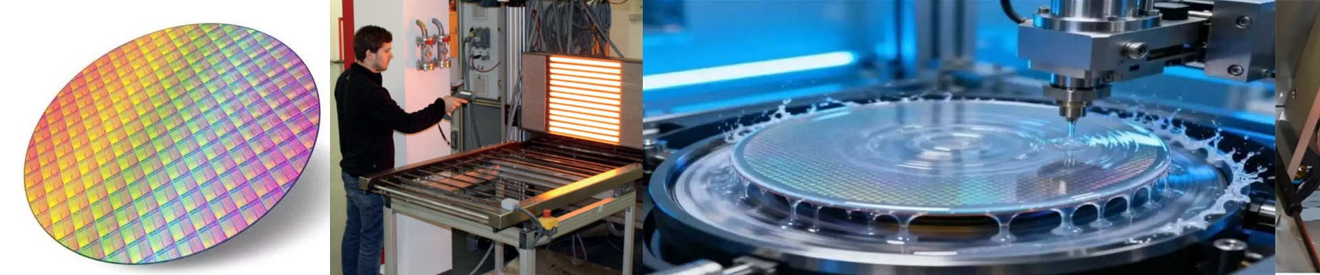
On the fab floor, a 0.5°C drift in the photoresist bake is all it takes to turn a good lot into scrap. Wafers sit and wait. Schedules slip. Particle counts climb. We built the semiconductor processing heater element to stop that kind of loss before it even shows up.
What matters, technically
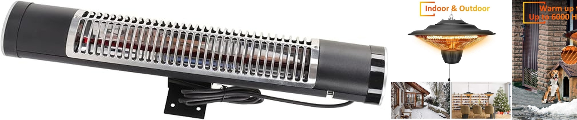
The heart of it is a quartz-based short-wave infrared heater, matched to the thermal budget of lithography and curing steps. Across the wafer, we hold uniformity within ±0.1°C, measured on-product with calibrated thermocouples. The emitters ramp fast and repeat tight, so soft bake and hard bake profiles stay locked in from lot to lot. The build is cleanroom-compatible, Class 1–100 rated, with low-outgassing materials and a geometry that doesn’t invite particles. That kind of construction keeps yields up where it counts.
Why it works in practice
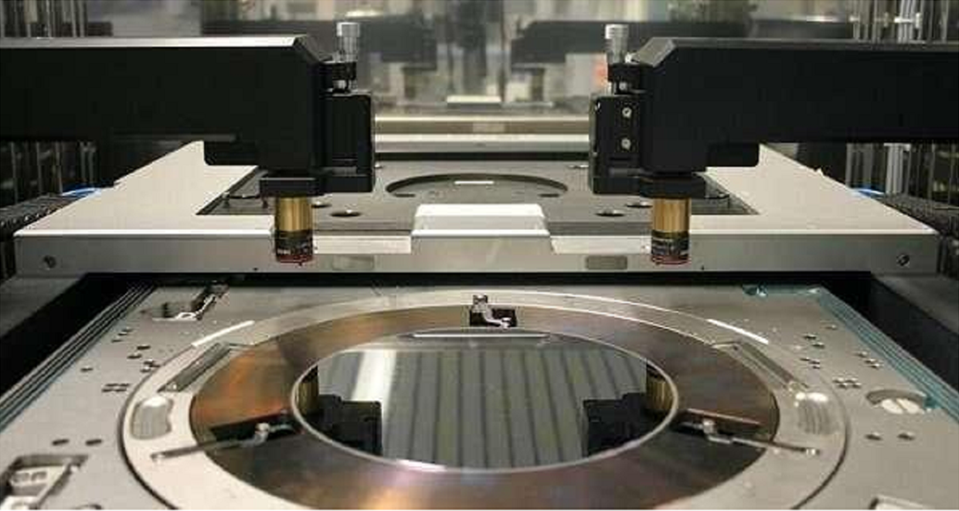
In photoresist processing, temperature uniformity directly drives CD control and line-edge roughness. Our heater element stabilizes the hot zone, cutting down within-wafer bias and cutting back on rework. Cleanroom compatibility and zero particle generation keep defect density down, while stable, repeatable cycles shorten time-per-wafer and trim energy use. You get fewer excursions, more predictable maintenance windows, and line yields that don’t swing around for no reason.
The things you need to know
Installation comes down to precise alignment to the process chamber and a verified thermal interface. The heater performs best when it’s matched to the chamber’s thermal mass and airflow; a mismatch will show up as uniformity drift. Plan on calibration every 2,000 hours and keep spare elements on the shelf—availability drops right when you need it most. We specify connector type, voltage, and dimensions so it integrates cleanly, but field fit is still a joint responsibility.