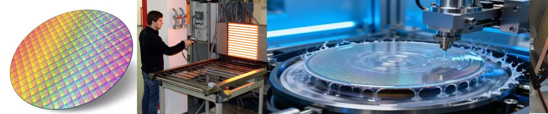
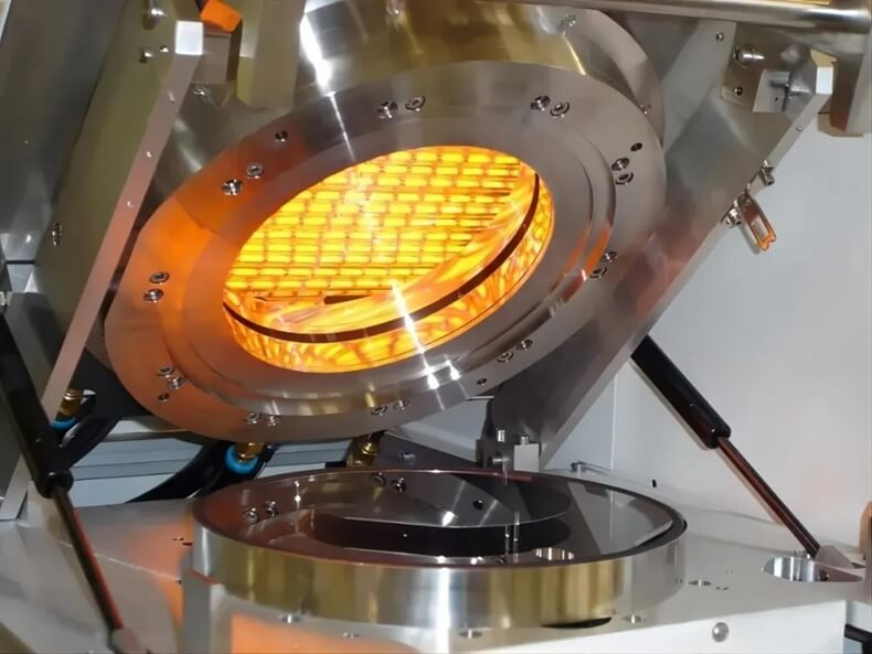
On the line, solder mask drying isn’t some gentle warm-up. It’s a boundary condition, plain and simple. A 1.5°C excursion will scatter thickness across the wafer, and the next lithography cycle grinds to a halt. If you’re running a zero-defect fab, that thermal tool has to act like a constant—not another variable to chase. What matters under the hood We built the system around short-wave infrared with quartz-halogen emitters, tuned to dump energy fast and keep it surface-dominant. Uniformity is the core requirement: ±0.1°C across the wafer during the solder mask bake window. Closed-loop control reads the film directly with calibrated pyrometry, not the chamber air, so the setpoint tracks what you actually care about. Cleanroom specs are Class 1–100, with low-outgassing materials and a laminar flow path that keeps particle generation at zero. Repeatability comes from recipe locking—temperature, time, and ramp rate—so every batch hits the same thermal budget, no guesswork. Why it holds up in practice This platform is engineered for the solder mask drying step right after coating, where you need moisture and solvent residuals gone—without stressing the film or triggering re-flow. The fast ramp shortens dwell time, which cuts the risk of native oxide before the next process step. When the bake is thermally repeatable, critical dimension control tightens and mask-related defects drop—meaning yield improves, directly. Energy use falls because you deliver heat on demand, instead of idling a heater and soaking the chamber. Fewer scrap lots, fewer reworks, and cycle time that behaves itself. What you need to plan for The system needs a cleanroom power and ground plan that matches its EMI profile, and the bake profile has to be matched to the specific solder mask chemistry. Commissioning is short—just enough to tune emitter power density and stage speed for your film stack. Once set, the process stays in control. But when you change the mask, the profile has to be re-verified. That discipline is the price of consistency.